Semiconductors
The semiconductor industry relies heavily on precise measurements throughout the entire process starting from initial research through process development to production of the final device. With the ever shrinking structure of features on chips, the requirements to measurement precision and resolution keep increasing. With its sub-nanometer resolution, its capability to deliver true topographic information, and the possibility to locally investigate electical properties of a wide variety of samples, AFM has become an indispensible tool in semiconductor industry and research.
Speak to an AFM Expert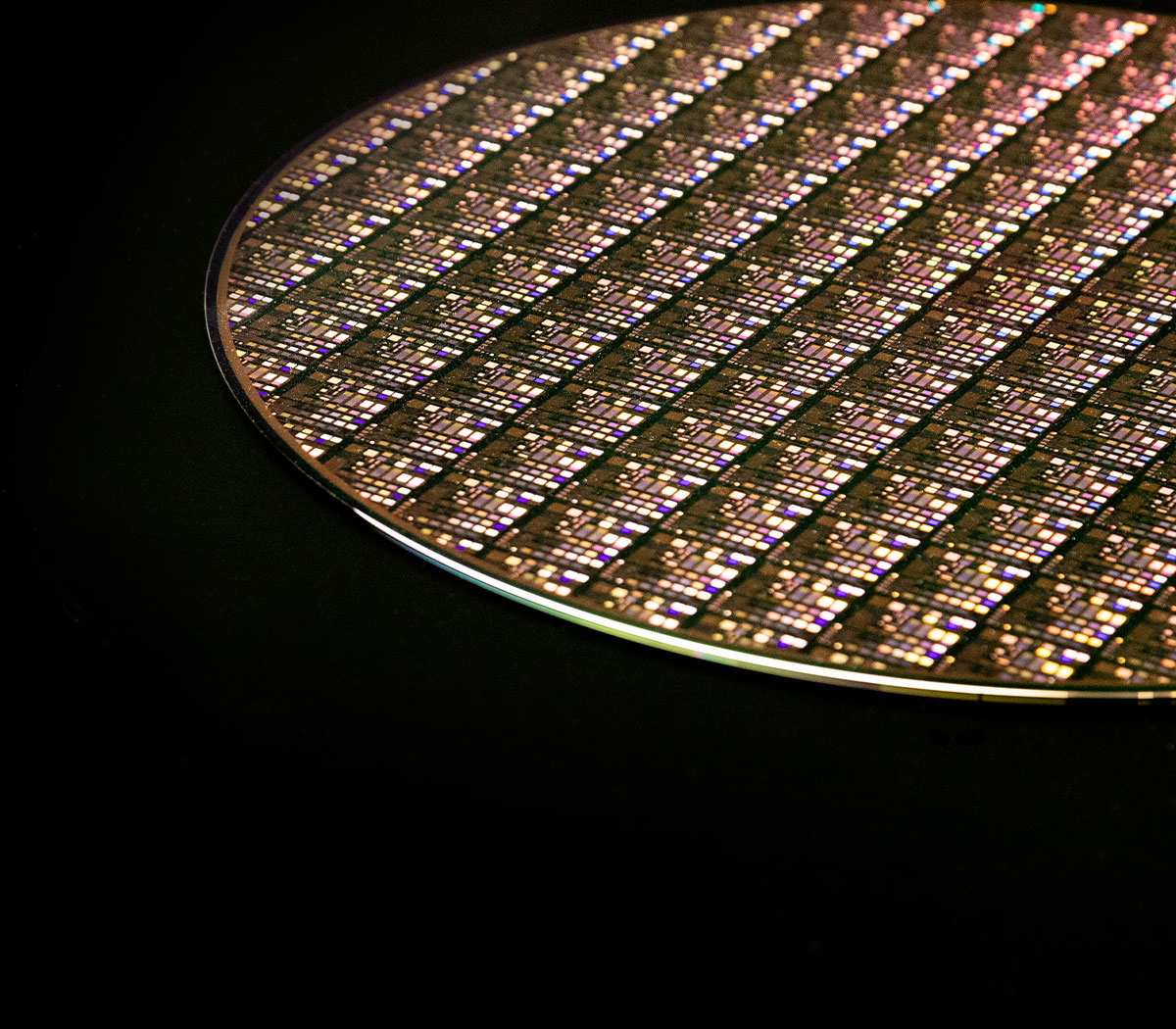
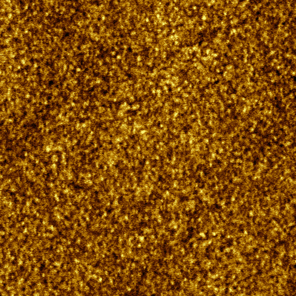
Wafer Roughness
With the continuous reduction in chip features, the importance of wafer surface roughness for yield and performance is heightened. Through the precision mapping of roughness at sub-angstrom levels, AFM provides semiconductor engineers with the tools to accurately quantify roughness, detect localized variations, and establish correlations with device behavior. This valuable insight enables the optimization of processes to achieve smoother surfaces, resulting in the production of superior chips.
Defect Review and Failure Analysis
In semiconductor failure analysis, Atomic Force Microscopy (AFM) has become an indispensable tool. Its exceptional high-resolution imaging capabilities allow researchers to visualize and characterize even the most minute defects on a semiconductor surface, defects that can have a catastrophic impact on device functionality. Moreover, specialized AFM modes can map the electrical properties of individual features, revealing variations in dopant density that can significantly influence device behavior. This comprehensive suite of functionalities empowers researchers to conduct in-depth investigations of defects and failures, ultimately leading to the development of more reliable and higher-performing semiconductor devices.
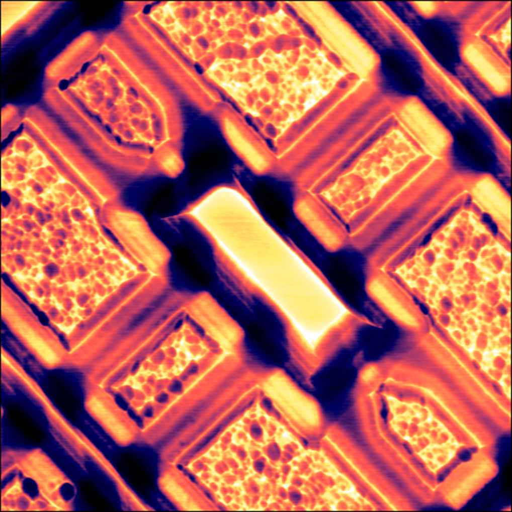
Critical Dimensions
As chip features miniaturize, precise control of critical dimensions (CD) becomes essential for integrated circuit function. AFM tackles this challenge by offering high-resolution, direct imaging of features on the wafer surface. Unlike traditional methods, AFM allows for non-destructive measurement of line width, spacing, and even feature height. This material-independent technique empowers engineers to ensure precise CD control across various layers in a complex chip, ultimately paving the way for high-performance and reliable integrated circuits.

Measurement Examples
#{ row.name }
There are no items to display.
#{ item.resourceType }
#{ item.date_text_field }
#{ item.name }
#{ truncateText(item.metadescription) }
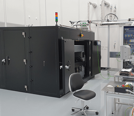
#{ item.readmoretext }Alphacen 300 Drive
Leveraging our proficiency in crafting industrial metrology systems, Nanosurf has introduced the Alphacen 300 Drive, a sophisticated AFM system tailored to satisfy the stringent requirements of the semiconductor industry. WaveMode enables the Alphacen 300 Drive to deliver fast, low-noise surface roughness measurements while addressing key metrology challenges in semiconductor production.
Industrial Solutions
Traditional tools for wafer analysis are crucial for evaluating wafer roughness, critical dimensions, and conducting failure analysis. However, the semiconductor industry's supply chain often demands alternative solutions for ensuring the quality of their products. This includes areas such as wafer production, cleaning and polishing technologies, and photolithography utilizing very short wavelengths ranging from DUV down to EUV.
Our team of skilled engineers understands this demand and is ready to support you with tailored characterization tools. We provide a range of automation and engineering services that go beyond standard system control and sample formats. Reach out to our Industrial Solutions team to discuss your specific measurement and analysis needs.
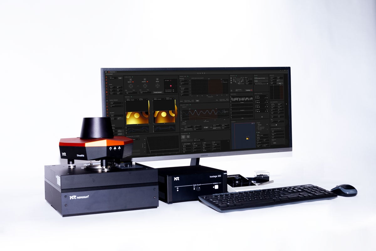
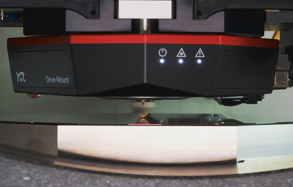
DriveAFM
The Drive AFM, featuring groundbreaking WaveMode technology and advanced electrical measurement functionalities, provides a robust toolkit for semiconductor research. Tailored for small samples, it serves as the perfect solution for early exploration of novel materials, structures, or processes before moving on to wafer-scale production. Its compact design also helps optimize lab space usage.