Electronics & Energy Materials
The AFM has quickly become an essential tool for researchers in electronics and energy materials fields. It unlocks information that is often difficult to obtain through other means. Whether it's a straightforward analysis of surface roughness and morphology or delving into the complex electrical properties of cutting-edge 2D materials or integrated circuits, AFM delivers an abundance of detailed insights at the nanoscale.
Speak to an AFM Expert
Battery Technology
Photovoltaics
Within the field of photovoltaics, AFM serves as a critical analytical tool for researchers seeking to optimize solar cell performance and durability. AFM's high-resolution imaging capabilities enable the characterization of surface morphology, a crucial factor influencing light absorption and charge transport within the photovoltaic material.. Furthermore, AFM extends its functionality to map the electrical properties of these materials. This comprehensive data set allows researchers to refine fabrication processes for solar cells, investigate material degradation mechanisms under environmental stressors, and ultimately guide the development of superior photovoltaic materials. Ultimately, AFM's ability to bridge the gap between structural and electrical characterization at the nanoscale positions it as a powerful tool for advancing next-generation solar cell technologies.
Electronic Devices
The relentless miniaturization of integrated circuits (ICs), the workhorses of modern electronics, necessitates ever-more sophisticated characterization techniques. AFM has emerged as a pivotal tool in this endeavor. Its exceptional resolution, reaching the angstrom level, allows researchers and manufacturers to assess surface roughness, precisely measure critical feature dimensions, and map the local electrical properties of the materials employed in ICs. This comprehensive data informs the development of fabrication processes, material selection, and ultimately, device performance. Additionally, AFM serves as a valuable tool for failure analysis, pinpointing the root cause of IC malfunctions and guiding further development efforts.

Thin Films and New Materials
Thin films, with their precisely engineered properties at the nanoscale, underpin a vast array of technologies. From integrated circuits (ICs) and displays to sensors, optics, and energy applications, their impact is undeniable. In photovoltaics, thin films play a crucial role in capturing and converting light into electricity, while in batteries, they contribute to efficient energy storage. Biomedical applications leverage thin films to enhance the biocompatibility of implants and facilitate targeted drug delivery. Additionally, they offer protective and decorative functionalities.
Atomic Force Microscopy (AFM) serves as an indispensable tool for the study and development of these versatile materials. Its capabilities extend beyond simple imaging, enabling researchers to analyze surface morphology, electrical properties, and nanomechanical characteristics. Furthermore, AFM allows researchers to investigate how thin films interact with their intended environments. By providing high-resolution data at the nanoscale, the very foundation of a material's behavior, AFM empowers researchers to understand and tailor thin films for their specific applications

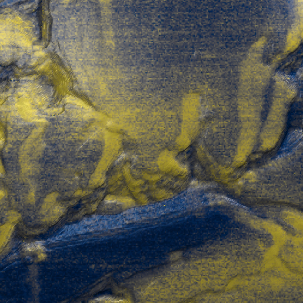
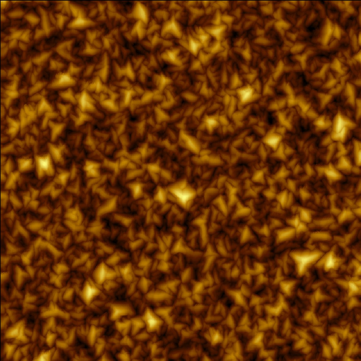
Measurement Examples
#{ row.name }
There are no items to display.
#{ item.resourceType }
#{ item.date_text_field }
#{ item.name }
#{ truncateText(item.metadescription) }
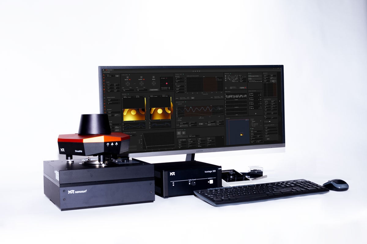
#{ item.readmoretext }DriveAFM
The DriveAFM, equipped with revolutionary WaveMode technology and advanced electrical measurement features, offers a reliable solution for conducting research on electronics and energy materials. Its ability to operate within a glove box enables the investigation of materials that require the precise environmental control provided by this setting.
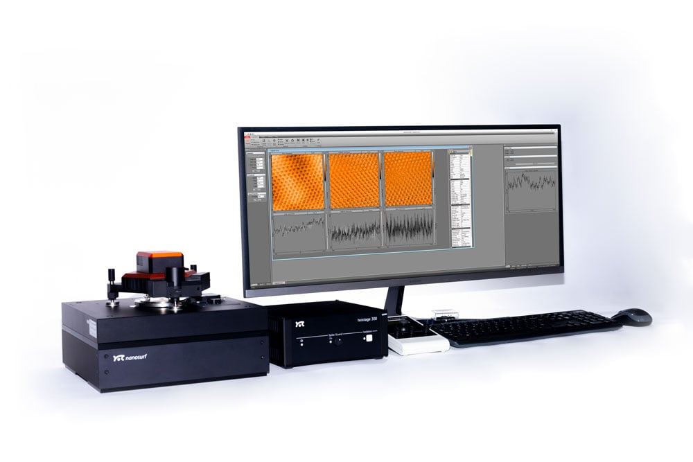
FlexAFM