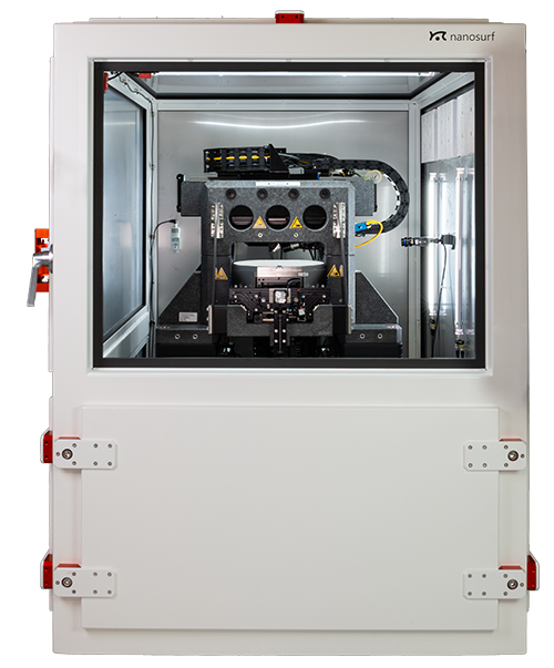
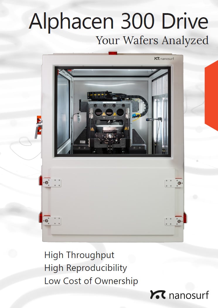
Alphacen 300 Drive
Your Wafers Analyzed
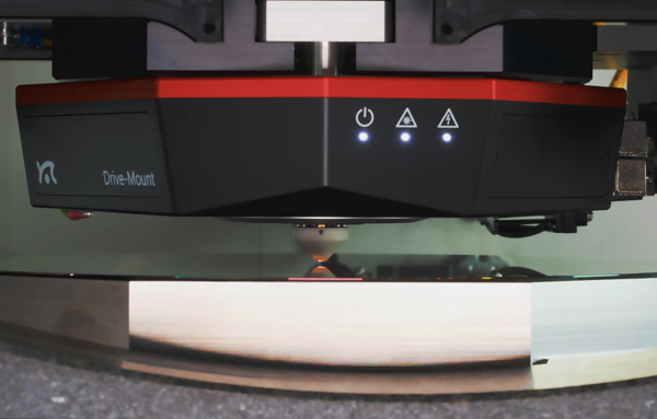
The Alphacen 300 Drive is an advanced atomic force microscopy (AFM) system engineered for 300 mm wafer metrology. Its precise tip-scanning platform delivers exceptionally low-noise, stable, and reproducible measurements. With WaveMode technology, the system achieves up to 15× faster line rates than conventional in-air AFM while preserving tip sharpness — enabling rapid, high-resolution analysis and consistent results, ensuring rigorous quality control in demanding semiconductor environments.
Speak with an Expert
Robust Surface Roughness Metrology
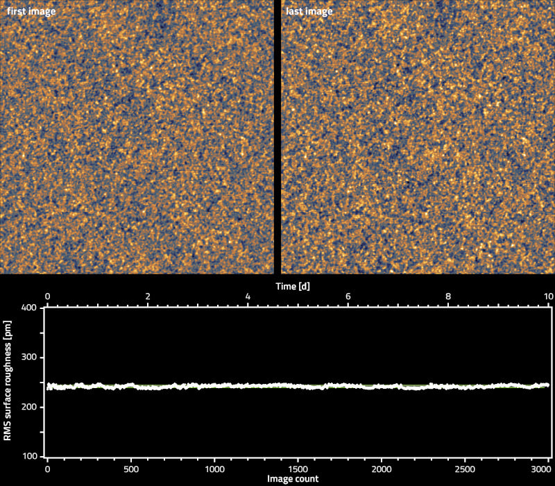
The Alphacen 300 Drive delivers highly reproducible, Angstrom-level surface roughness metrology, achieved through advanced stage engineering and WaveMode—Nanosurf’s photothermal off-resonance imaging technology. WaveMode ensures consistently low, quantitative tip-sample interaction forces during imaging, maintaining tip sharpness over extended use. This robust performance supports user-friendly operation and minimizes total cost of ownership.
Image: Time-series of surface roughness measurements of a silicon wafer using WaveMode. Images in the top row show images at the beginning of the series and after 10 days. The graph below shows the roughness determined from each image of the series.
Ultra-Stable Stage Design
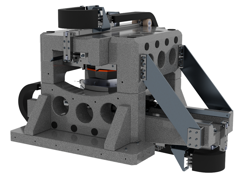
The Alphacen 300 Drive is designed to ensure reliable measurements, even on ultra-smooth surfaces. Its ultra-stable stage provides low noise, high stability, and sub-micron positioning accuracy to meet the requirements of complex sample analysis. Based on more than two decades of experience in industrial stage engineering, the system offers the rigidity and performance necessary for high-performance AFM metrology.
Automation
The Alphacen 300 Drive is equipped with automation features to streamline measurement workflows. Automatic wafer and cantilever alignment, and support for KLARF file-based routines increase operational efficiency. The programmable 300 × 300 mm² sample stage, together with WaveMode technology, ensures precise and consistent measurement of surface roughness and dimensions across the full wafer area.

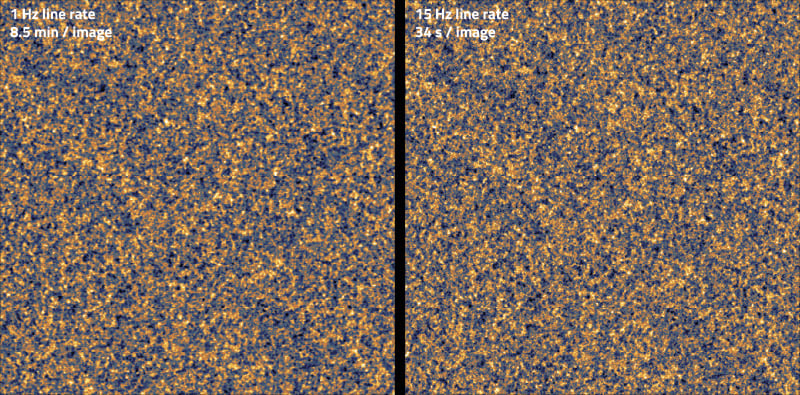
Fastest Angstrom-Level Surface Roughness Metrology
Faster yet accurate assessment of surface roughness is achieved with WaveMode, which overcomes the limitations of conventional in-air imaging modes and substantially increases imaging speed.
Image: Comparison of silicon wafer surfaces acquired at the standard 1 Hz line rate and at the 15 Hz line rate achievable with the Alphacen 300 Drive.
Wafer Edge and Sidewall Inspection
The new wafer edge and sidewall inspection approach delivers detailed information on sidewalls and wafer edges from the top surface down to the apex, with sub-nanometer resolution. High-resolution wafer edge profiles and images reveal critical, previously unobserved regions of the wafer, providing new insights for process control and optimization.

Download the Alphacen 300 Drive Brochure
The PDF brochure includes details on the Alphacen 300 Drive technology, application examples for different areas of interest and system specifications.
Example Measurements
#{ row.name }
There are no items to display.
#{ item.resourceType }
#{ item.date_text_field }
#{ item.name }
#{ truncateText(item.metadescription) }
#{ item.readmoretext }Interested in Alphacen 300 Drive?
Get to know the Alphacen 200 Drive! Reach out to us to discuss your application with one of our seasoned AFM experts, to get a budgetary quote or schedule a product demonstration or exploratory meeting.