Wafer Edge and Sidewall Inspection
Nanosurf’s wafer edge and sidewall inspection solution is the first to characterize both vertical and horizontal surfaces without changing the probe or tilting the sample or scan head. It delivers precise edge metrics and high-resolution topography from the top surface to the apex, helping semiconductor manufacturers detect edge defects that lead to yield loss.
- Unlock quantitative profile metrics such as radius or bevel angle
- Inspect and gain insights on edge defects
- High-resolution surface roughness from the top surface to the apex
- Optimize processes and thus yield by reducing wafer loss during production

Why Wafer Edges Matter
Sidewall imperfections - such as roughness, undercuts, or residue accumulation - spanning from the top edge through the complex bevel geometry to the apex directly cause particle shedding, film delamination, and significant yield loss in advanced packaging, 3D NAND stacking, and wafer production. These defects propagate contamination across frontside and backside surfaces, exacerbated by non-uniform deposition, etching processes, and wafer ellipticity under high film stress, leading to excursions during technology ramps. In hybrid bonding, sidewall roughness reduces effective contact area and bond strength, resulting in voids and reliability failures, while in photonics, it induces light scattering that degrades waveguide efficiency and optical coupling. Additionally, poor edge profiles heighten chipping, breakage risks from gripper contact, and handling issues, undermining throughput and device performance at sub-2nm nodes.
The Comprehensive Solution - AFM-Based Inspection
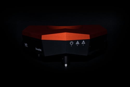
Nanosurf’s Edge and Sidewall Inspection introduces a new AFM-based technique that enables reliable tracking of surfaces, including vertical structures. Leveraging the inherent stability of tip scanning and photothermal excitation, and combined with the ultra-low-noise architecture of the DriveAFM, this approach ensures precise localization of surface features in three-dimensional space across a wide range of geometries.
A key advantage of this technique is the ability to characterize both a horizontal surface and a vertical sidewall, including roughness and critical dimensions, using a single AFM probe and without tilting the system. Because no tilt is required, the sample stage maintains the stability necessary for high-speed roughness measurements, allowing the same system to be used efficiently for wafer roughness characterization and sidewall inspection.

Wafer Edge Profiling
Accurate characterization of the wafer edge profile - including radius or bevel angle - is essential throughout all wafer processing steps, from deposition and etching to hybrid bonding and handling, as suboptimal profiles lead directly to yield loss. Nanosurf’s AFM-based edge and sidewall inspection provides true nanometer spatial resolution across the complete edge profile, from the top surface to the apex, and quantitatively captures profile features that remain inaccessible to optical or stylus profilometry. This AFM performance enables precise defect root-cause correlation and process optimization that are not achievable with other inspection methods.

Surface Roughness and Topography Across the Whole Profile
AFM-based metrology is indispensable for quantifying nanoscale surface roughness (Ra, Rq) on the wafer edge bevel and apex, where excessive peaks, nodules, or valleys trap particles and residues from etching/deposition processes, causing shedding that contaminates frontside/backside and triggers yield-killing defects in 3D NAND, advanced packaging, and photonics. Unlike optical tools, AFM delivers sub-nm resolution to precisely measure these critical regions ensuring process optimization and edge die yield boosts.

Sidewall Metrology brochure download

Automated Profiling
Optimized for autonomous operation, the wafer edge inspection solution can be carried out by the AFM system without the supervision of a technician. Increasing characterizing yield and enabling continuous operation.
Time-lapse of automated wafer edge profile creation

