FlexAFM and nanomotion sensing unveil cellular responses, offering new insights into bacterial behavior and potential ...

15.03.2024

Héctor here, your AFM expert at Nanosurf calling out for people to share their Friday afternoon experiments. Today I show you how stick-slip is your friend to perform conductive AFM on atomic lattice.
Imaging atoms, or atomic lattice, can be interesting for a number of reasons, but sometimes setting up things can be tricky, so as I did with the post about torsional resonance, I want to give you some tips and tricks to make your life easier (remember always to practice, and go from the known to the unknown one step at a time).
We will be looking at HOPG, which is a common sample found in many AFM laboratories. Its advantages are that it is conductive and that using a cell tape you can easily cleave it creating a fresh new surface each time.
The imaging mode will be static force, meaning that the deflection signal is used as feedback. For the probes used here (Tap 150 and Multi 75E), the setpoint was in the range 10 - 300 nN, the imaging range 10 nm, and the scan speed around 40 Hz at 512 pixels.
OK OK, but how do I know If I'm looking at atoms or simply noise? Here the stick-slip mechanism is your friend.
The stick-slip mechanism consists in your probe moving in a short of jumpy way. It sticks to one position, then you pull and suddenly it jumps to a new position. You monitor this movement with the lateral signal, and as explained on the torsional mode post, this increases the lateral sensitivity.
OK, my signal is periodic and looks like jumps, is it atoms or atomic lattice? There are two ways of checking it, one is to zoom in or zoom out, the other one is to measure conductivity.
The nice part of conductivity, is that unlike deflection, which is somehow similar to the lateral signal (for some scan directions at least), conductivity will be very different, and in principle its resolution should be even better than lateral.
Everything sounds nice and simple, but is it really that simple? Well, for this fridayAFM I got some help and managed to record the whole process.
You forgot to tell us the gains and where to put the lasers. Yes... and now. I used the default gains for static, and the laser position given by the automatic laser alignment. Where is the trick then? On a low noise floor on the lab (although you can hear it is an acoustically noisy lab), on a sample firmly attached, and thermal equilibrium (the longer you let the sample and AFM rest, the better imaging quality).
I have to admit that having the right probe helps a lot. Above you can see that the Tap 150 is struglling a bit, while below you can see much nicer images taken with the Multi 75E.
Two things to point out. One is patience, as shown on the video, sometimes it takes a few scans for the probe and surface to clean.
The second one is to try several scan directions. As you can see below, the shapes shown on the conductive signal change a lot when changing the scan direction (all these images where taken with the same probe, simply imaging along different directions).
But if everything changes with direction, how can I optimize my scan parameters? Well, it turns out that the lateral signal doesn't change that much, and remains high (unlike the deflection, which almost vanishes for certain scan directions). You can see that below.
Let's recap. We imaged HOPG atomic lattice, showing how the deflection, the lateral, and conductivity looks like. In particular, we showed this for two probes (one not so good), and for several scan directions to highlight how the contact area changes the shapes seen in the conductivity images.
I hope you find this useful, entertaining, and try it yourselves. Please let me know if you use some of this, and as usual, if you have suggestions or requests, don't hesitate to contact me.
Further reading:
Exploring Nanoscale Organization of Normal Alkanes on HOPG Substrate with DriveAFM
Unveiling the Power of Electrical Modes
[1] Berman, Alan D., et al. Origin and Characterization of Different Stick−Slip Friction Mechanisms, Langmuir 1996, 12, 19, 4559–4563, https://doi.org/10.1021/la950896z
Almost forgot. Some images where too large to be cropped onto the figures...
23.06.2026
FlexAFM and nanomotion sensing unveil cellular responses, offering new insights into bacterial behavior and potential ...

27.05.2026
Explore Alejandro Silhanek’s innovative spintronics research, showcasing how spin waves can be investigated leveraging ...
.jpg?width=330&height=330&length=330&upsize=true&upscale=true&name=Mayfield%20Girls-202581%20(1).jpg)
19.05.2026
A group of young girls from Mayfield school wanted to start a F24 electric car racing team, and Nanosurf decided to ...

08.12.2024
Learn how to make a Python code to interface your AFM with a gamepad.
01.10.2024
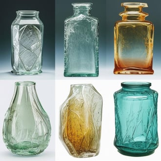
Discover how different types of glass age and degrade over time, and learn how to use AFM technology to investigate ...
11.07.2024
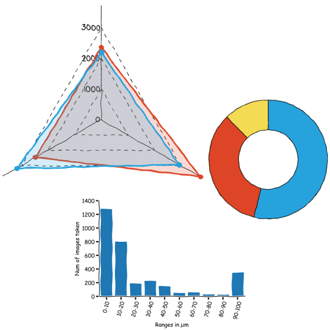
FridayAFM: learn how to perform datamining on large sets of AFM data.
Interested in learning more? If you have any questions, please reach out to us, and speak to an AFM expert.