Discover the capabilities of WaveMode AFM in characterizing bottlebrush polymers with unprecedented detail and speed, ...

12.01.2024

Héctor here, your AFM expert at Nanosurf calling out for people to share their Friday afternoon experiments. Today I investigate an unknown sample with microwave microscopy.
If I trained you on the use of AFM, at some point or another you heard me saying:
“do small steps, try to go from a known sample to an unknown one using a semi-unknown sample in between”.
This is something I follow myself, and is why sometimes I propose basic samples for fridayAFM, (and try revisiting them with new experiments as often as possible).
Ink is one of those samples. Ink has been part of a couple of fridayAFM experiments so far because it can be applied to many different surfaces, it forms nanostructures, and it doesn’t increase the roughness of the surface too much.
For instance, some time ago I imaged how ink changes the surface of paper and covers it with tiny micro-spheres.
Then I used it on egg membrane to see if I could detect spheres deposited on top of the membrane fibers (before trying to deposit yeast on the same membrane).
So, today ink will help me on learning a bit more about scanning microwave microscopy (SMM for short).
At home I found this set of metallic color pens. Apparently, from the descriptions I could find, the metallic finish is given by metallic flakes added to the ink. These flakes are in suspension with the ink, and once the ink dries they remain on top of the painted surface reflecting light in such a way that resembles a metallic surface.

In other words, this ink should provide me with a surface with particles with low and high impedance, a nice test sample for SMM. So I started by painting a glass slide with the markers. By the way, glass is a surface that we know pretty well also. We tried cleaning glass in the past.
and also tried coating it to change its wettability.
In other words, we know how the glass looks like, how the ink looks like, and the only unknown should be the metallic flakes (if there are any). Can we see the metallic flakes? Not on the topography, at least to me they don't seem evident.
Can the SMM help us?
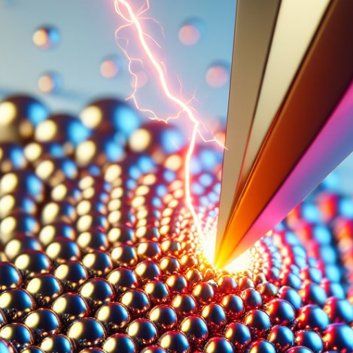
The SMM system operates by sending a radiofrequency signal through the probe down to the sample surface. The ratio between the generated signal and the reflected signal is proportional to the conductivity of the surface.
How the reflected signal is generated? When transmitting microwaves, each interface is a source of impedance mismatch, which means that each interface splits the incident wave onto a transmitted and a reflected wave. This is true for all the elements in the circuit, including the probe-surface interface. So, as the probe moves the coupling changes and the amount of reflected signal changes in response to changes in the surface.

Now, why the resonator in the circuit, and why the title of this post? As I said, each interface adds new waves to the circuit, the purpose of the resonator is to select some of those frequencies and null the others (or more precisely, let them decay). But the resonance of the circuit is dictated not only by the resonator but also by all the interfaces... which means, that in order to have the maximum sensitivity... we have to tune the frequency of the generated signal to match the resonance of the whole thing, and today for this experiment... it was 4866 Hz.
So, how the ink looks like in terms of microwave absorption?
Microwave absorption lets us see the metallic flakes easily. They shine in bright colors in the absorption maps. We can see that they tend to have about 10-20 μm in size and that they are quite dispersed (at least in the green ink, on the grey they seem buried).
What is more interesting, is that in some cases the drying process seems to have drifted the flakes towards the edge of the drying ink, while in others the distribution is quite homogeneous (think about this when doing small scan ranges and not finding anything).
One open question: there seem to be many particles with low conductivity (i.e. dark), are they made of different material or the same material but just different structure? Like for instance, hollow capsules, or filled with solvents... For now I have no answer.
Let's recap. Metallic ink seems an interesting test sample for SMM. There are a few open questions, like what are the low conductivity parts, and what is the composition of the metallic flakes, but if all that maters is testing the contrast of the system (to see if is has been tuned properly), then this is a suitable sample. Additionally, we learned a little bit more about ink, which is likely to be useful in the future.
I hope you find this useful, entertaining, and try it yourselves. Please let me know if you use some of this, and as usual, if you have suggestions or requests, don't hesitate to contact me.
Further reading:
Application note: Unveiling the Power of Electrical Modes.
Application note: Scanning Microwave Microscopy for the Semiconductor Industry
28.10.2025
Discover the capabilities of WaveMode AFM in characterizing bottlebrush polymers with unprecedented detail and speed, ...

27.10.2025
Read this blog and discover advanced alloy engineering and cutting-edge AFM techniques for high-resolution, ...

14.10.2025
Discover how WaveMode technology resolves the tobacco mosaic virus structure under physiological conditions with ...

08.12.2024
Learn how to make a Python code to interface your AFM with a gamepad.

01.10.2024
Discover how different types of glass age and degrade over time, and learn how to use AFM technology to investigate ...

11.07.2024
FridayAFM: learn how to perform datamining on large sets of AFM data.
Interested in learning more? If you have any questions, please reach out to us, and speak to an AFM expert.