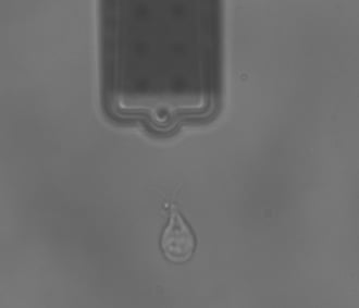
How to measure mechanics of single cells
06.10.2023

Héctor here, your AFM expert at Nanosurf calling out for people to share their Friday afternoon experiments. Today I look at the surface potential in a sample with phosphorescence.
More precisely, I use an old clock to see how phosphorescence and UV lighting can affect surface potential. For those not familiar, surface potential is linked to the surface work function in the easiest cases (how much energy it takes to extract one electron from the surface and send it away), and with trapped charges in the most difficult cases.
Why I want to do this? Why not? I mean, I used to work on calibration of Kelvin-probe force microscopy (KPFM), and this could be an interesting effect to either aid with calibration of KPFM at nanoscale, or to take into account when coming up with the absolute value. In both cases, it could be cool to gather some data and see if there is anything to it. If you are still not convinced how cool it is, I was looking at articles like Ref 1, where KPFM is combined with light to measure charge accumulation, so there it is, forefront of science and all.
The idea is simple (see bottom left diagram of the figure above) surface potential depends on where the electrons are sitting within the atom (i.e. the Fermi level). If the electrons move to the top energy levels (e.g. when the temperature raises), the Fermi level changes and as a result the surface potential of the sample changes. In the phosphorescence effect (also in the same panel), light excites electrons to a higher level, they stay there some time changing between different spin states... and eventually they decay emitting light with longer wavelength than the original one (see Ref 2 for more details). Thus phosphorescence is somehow similar to raise the temperature, and thus, it should also affect the Fermi level.
Now, not all electrons on an atom will react this way, for starters they are in different energy levels, and not all atoms within a sample will react at the same time... so the effect is ought to be tiny even in phosphorescent materials with long decay, because at a given time only a fraction of electrons will be in the excited state, but... can we see it with KPFM?
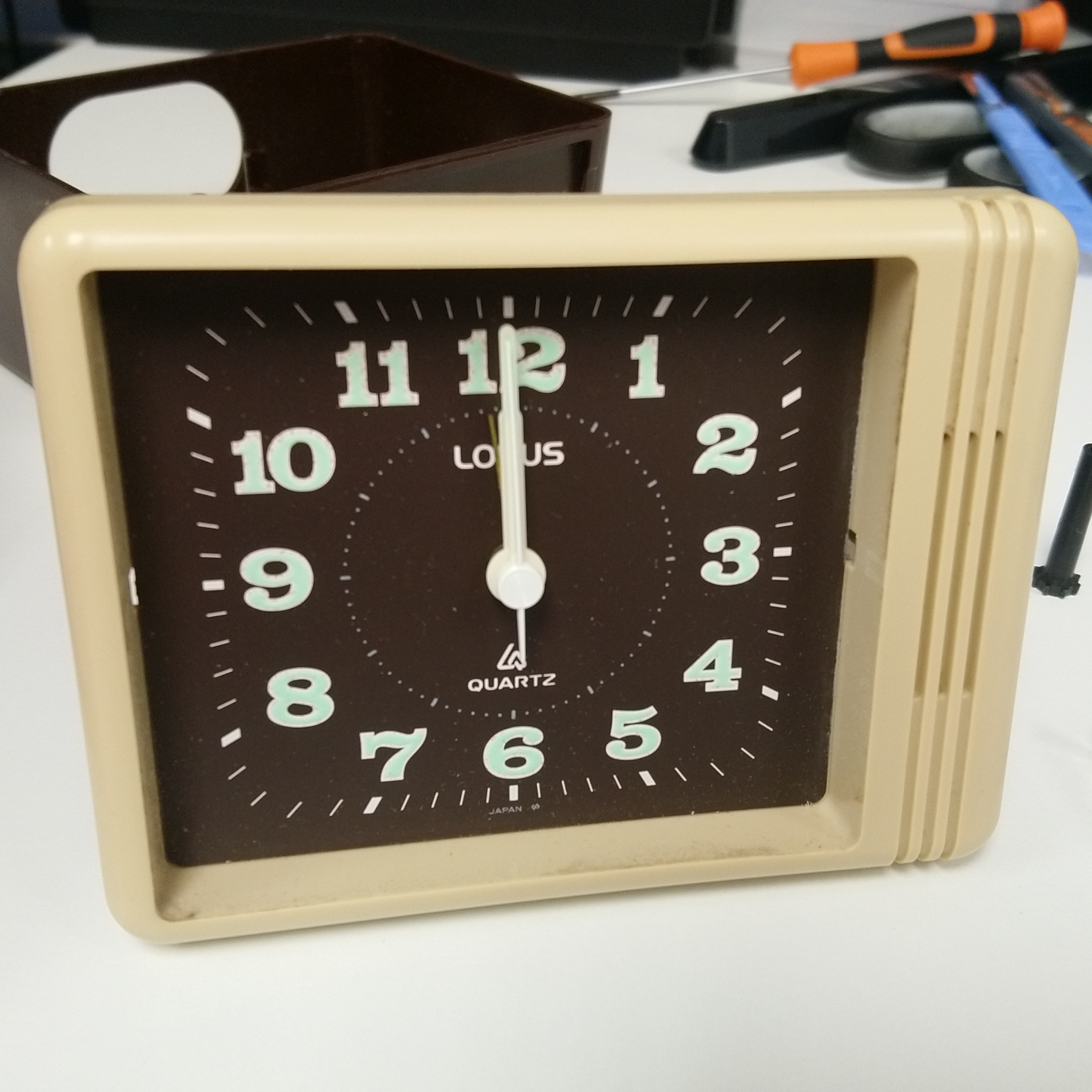
To test this I got myself an old clock (there are two reason for looking for an old clock, one is that it is cheaper than a new one, and second reason is that I was somehow hoping I will get one with radioactive material on the paint). But I was not so lucky. This clock was probably built between 1960-1970, and according to Wikipedia, phosphorescent paint replaced radioactive material with zinc sulfide in the 1930s, and zinc sulfide was replaced with strontium aluminate in 1993.
Nevertheless, as you can see in this video, my clock has quite good phosphorescence, and it is easy to disassemble, so I will not complain about not getting the radioactive material.
Now, the setup I prepared is quite simple (hey, don't laugh, if it looks silly but it works, it is not silly). The sample is holded onto the stage with clips, and the stage is grounded. Note that the paint is applied on a metallic support, this will help minimizing capacitive effects. I attached an UV flashlight to a stand and I turn it ON/OFF manually. Everything is enclosed inside of the acoustic hood. So, it is dark inside unless I turn the UV flashlight ON.
So, what we see? Lots of stuff. It is actually quite difficult to pinpoint which parts are producing the phosphorescence, because there are lots of different structures inside of the painted area (it seems it was quick and dirty job back in the days). Luckily, zinc sulfide tends to form either cubic or hexagonal crystals, and as you can see, those are very easy to spot.
I actually liked so much the geometrical shapes that I took some extra images (to be honest, I always take a lot of images, to make sure the imaging conditions are stable, that I can reproduce results, and that the area I show is representative of the whole sample and not a lucky find).
Talking about lucky finds, if you compare the topography and phase images below, you will notice that although in topography all the crystals seem the same, in the phase we can clearly see that some crystals have residue over them. Not sure what it is, but since only few crystals have it, I'm going to asume it is contamination or fabrication residue.
Now for the UV part of the experiment. The idea here is to measure surface potential in the dark, measure again with UV illumination, measure again in the dark... and repeat.
For this part, I made sure the sample was in the dark for about one hour and then imaged it in dual pass using amplitude modulated 2nd harmonic KPFM to detect the surface potential (for those not familiar with the different KPFM modes out there, I recommend my colleague Amelie publication in Ref 3). If I can use single pass, I tend to prefer it as quicker, however, in this case, the high topography meant that I can easily have topography cross-talk onto the surface potential, and thus, to avoid any risks, a second pass technique was advisable. As a rule of thumb, always look at the phase during your first pass, if there are big changes (e.g. 90 deg), your are likely to have topography artifacts in your surface potential.
Here are the results:
Are there changes? Yes. Are they tiny? Absolutely.
There is a visible effect from the UV light, and we can see this and rule out drift in the measurement because after turning the UV off, the values go back to where they were (these images here and the values are raw, they haven't been flattened in any way). What I didn't anticipate is that the "UV" electron pumping will happen also in every other material not just the phosphorescent, and thus, both background and AFM probe have their surface potential shifted.
Is this effect of the phosphorescence?
I see several possibilities here:
Can you think of more explanations? (help please)
In any case, I hope you like the results shown, with or without explanation I think they are cool, and sometimes it is like this, there is only time and resources to explore a bit.
Ah! Almost forgot it. Can we repeat it? This below is a different probe, on a completely different area (images before where on number "5", this here is on number "6" of the clock panel). Judge by yourselves.
References:
1 Bergmann, V., Weber, S., Javier Ramos, F. et al. Real-space observation of unbalanced charge distribution inside a perovskite-sensitized solar cell. Nat Commun 5, 5001 (2014). https://doi.org/10.1038/ncomms6001
2 Massimiliano Malgieri et al. Looking at phosphorescence with a smartphone, explaining phosphorescence with a dice toy model 2018 Phys. Educ. 53 065016 doi:10.1088/1361-6552/aaddf1
3 Axt, A.; Hermes, I. M.; Bergmann, V. W.; Tausendpfund, N.; Weber, S. A. L. Know your full potential: Quantitative Kelvin probe force microscopy on nanoscale electrical devices. Beilstein J. Nanotechnol. 2018, 9, 1809–1819. doi:10.3762/bjnano.9.172
4 Matthias Zorn, Stefan A. L. Weber, Muhammad Nawaz Tahir, Wolfgang Tremel, Hans-Jürgen Butt, Rüdiger Berger, and Rudolf Zentel. Light Induced Charging of Polymer Functionalized Nanorods Nano Lett. 2010, 10, 8, 2812–2816 https://doi.org/10.1021/nl100741n
06.11.2024
How to measure mechanics of single cells
14.05.2024
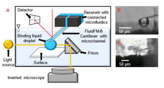
How to measure forces between droplets
11.03.2024
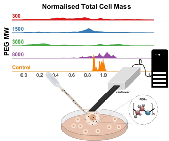
How to perform mass measurements in cell exposed to different environments.

08.12.2024
Learn how to make a Python code to interface your AFM with a gamepad.

01.10.2024
Discover how different types of glass age and degrade over time, and learn how to use AFM technology to investigate ...
11.07.2024
FridayAFM: learn how to perform datamining on large sets of AFM data.
Interested in learning more? If you have any questions, please reach out to us, and speak to an AFM expert.