Discover the capabilities of WaveMode AFM in characterizing bottlebrush polymers with unprecedented detail and speed, ...

22.09.2023
Héctor here, your AFM expert at Nanosurf calling out for people to share their Friday afternoon experiments. Today I do some computer-age archeology. #industrialarcheology #digitalarcheology
This friday AFM was going to be about checking a light detector (CCD detector) with a microlens array. I wanted to show what it looks like, and collect data for a project about measuring the evolution of sensor sizes throughout the years. However, I found that the available documentation is not clear about the sensor structure. So, I decided to turn it into an industrial archeology project.
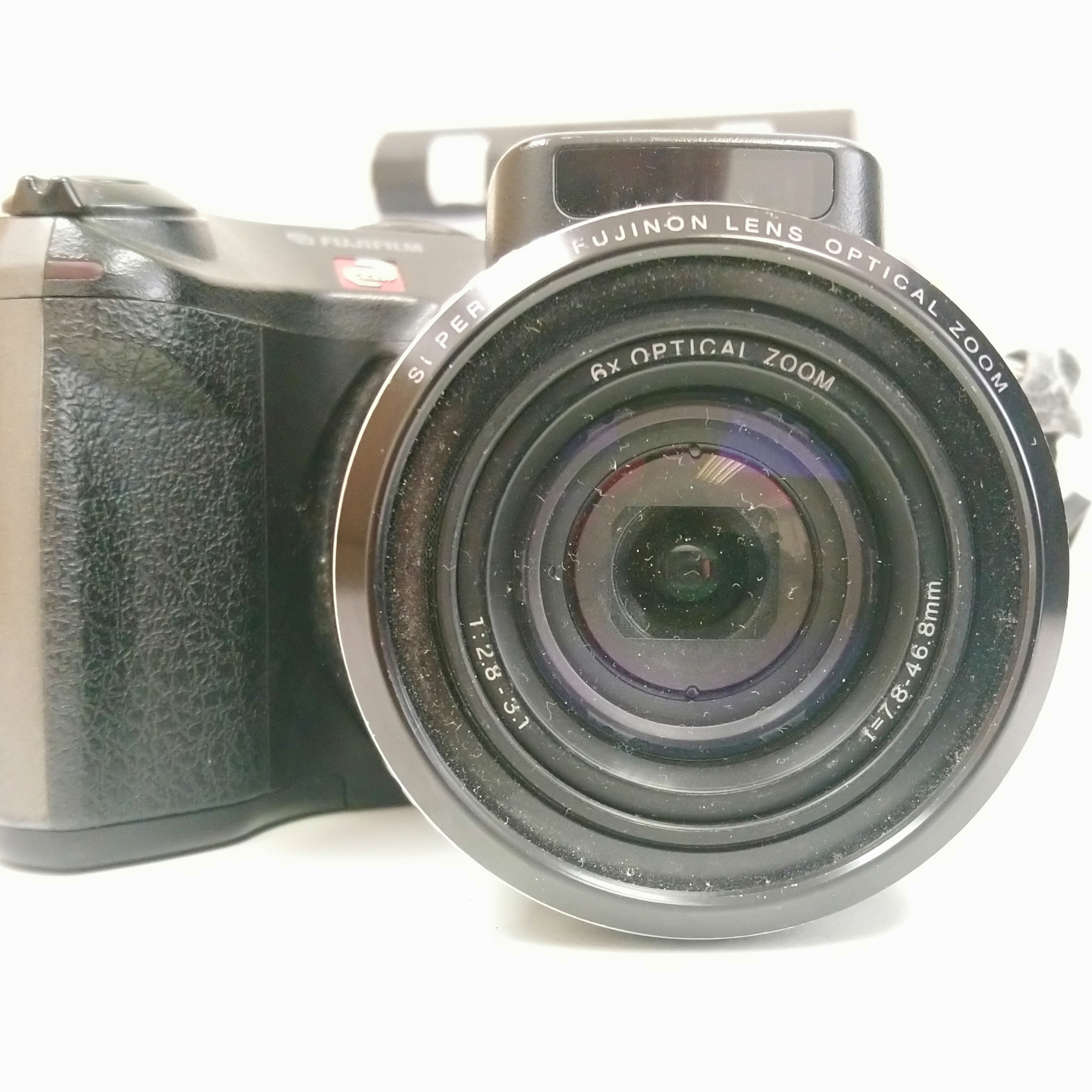
The camera I disassembled was a Finepix S602 Zoom from the year 2002. I used to own this model back in the day, so when I saw it for sale a few years ago, I bought it... and used it until nostalgia alone couldn't justify keeping it anymore.
It is not the first camera I disassembled, and I knew what I was in for, but I have to admit that it always impresses me how many parts they have, and in particular, that the CCD is almost the last thing that comes out. In any case, I disassembled it and I had the photodetector.
Now, according to this Wikipedia article the sensor is a Super CCD III, but there is no more reference there about what a SuperCCD III is.
SuperCCD, according to Fujifilm promotional material from 2002 (from this e-paper stored in Yumpu), consists on imaging sensors with three layers, octagon-shaped photodetectors, color filters, and microlens array. But there is no link to second or first generation. Is the octagon the distinctive feature of the third generation or is something else and that feature was already present in previous generations?
To help clarify these questions a little bit more, there is this Wikipedia article on Super CCD. From it it becomes clear that the octagons and the 45 deg arrangement of them is the key feature of the term Super. But unfortunately, this article jumps generation III, leaving with the question if generation III consists of octagons or, as depicted in the "classique", is made of square detectors.
But luckily for us, there is another source, which brings more clarity. The answer came from this personal blog (translated from German). Where it clarifies that Gen III is with octagon-shaped elements, and each octagon is a single photodetector. In Gen IV additional detectors were added.
So, now it is time to check if it is true the conclusion we came up with.
First of all, the next figure is a summary of all we know, plus a complete optical view of the chip. It is interesting to note the filter marks on the top right corner (I assume this is for QC to be check at the end of the fabrication procedure).
Note: The microlenses part is very difficult to image, and depending on the illumination and the color valance, it can be highlighted or darkened to see other areas of the chip.
For the AFM imaging (shown below), the chip was resting in the sample stage with clips to fix it in place. The only difficulty is that the chip is surrounded by hard plastic walls, and the access inside is limited. However, imaging towards the centre, were the probe holder fits, is fine.
First thing to check is if the probe fits in between the microlenses, and the answer is yes, it does: the smallest gap in between lenses forms a 108 degree angle, while the maximum tip angle for the Multi 75 probes is 60 degrees.
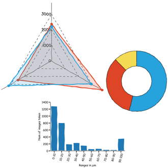
With the knowledge that the probe can resolve the features without a problem, imaging the microlenses is straightforward. From there it is possible to extract a pixel size of 7.78 by 7.78 μm2.
Next, to check which version of the Super CCD it is, I scratched the surface with a knife. This revealed two types of surfaces, one that is likely to be the filters, and another one, underneath, that is likely to be the photodetectors exposed. This conclusion is supported by the fact that in the image in the middle (the one that is likely the filters), the elements touch each other (which is OK, because there is no electricity involved). On the right image however, elements are clearly separate, as expected with electrically active elements, because if they touch there could be crosstalk.
So? So the conclusion is that this is a Super CCD Gen III, each cell is an octagon and each cell is a single photodetector.
Last minute addition!
My colleague Hans has been very kind donating his computer and performing some measurements on the camera... which allows me to show you this graph on pixel size evolution over the years (I know calling it graph is a bit ambitious, but don't worry, it will get populated in subsequent fridayAFM experiments). Interesting to note that the three data points align pretty well in logarithmic scale (as predicted by Moore's law).
Hopefully, you liked this bit of industrial/digital archeology research, and maybe discovered something new about everyday objects. I promise to have a follow up on the pixel area graph with more data points. Stay in touch, and if you have more info, please share.
Extra: After further inspection, I notice this change in the background around the border of the microlenses area. Could it mean that several rows at the border of the chip are not being used or have a different purpose than imaging?

28.10.2025
Discover the capabilities of WaveMode AFM in characterizing bottlebrush polymers with unprecedented detail and speed, ...

27.10.2025
Read this blog and discover advanced alloy engineering and cutting-edge AFM techniques for high-resolution, ...

14.10.2025
Discover how WaveMode technology resolves the tobacco mosaic virus structure under physiological conditions with ...

08.12.2024
Learn how to make a Python code to interface your AFM with a gamepad.
01.10.2024
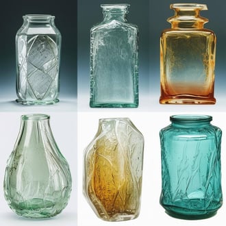
Discover how different types of glass age and degrade over time, and learn how to use AFM technology to investigate ...
11.07.2024
FridayAFM: learn how to perform datamining on large sets of AFM data.
Interested in learning more? If you have any questions, please reach out to us, and speak to an AFM expert.