FlexAFM and nanomotion sensing unveil cellular responses, offering new insights into bacterial behavior and potential ...

22.03.2024

Héctor here, your AFM expert at Nanosurf calling out for people to share their Friday afternoon experiments. Today I show you how to make a point-contact diode out of a galena crystal.
1874 Ferdinand Braun, at Würzburg University, probed a galena crystal (lead sulfide) with the point of a thin metal wire. Braun noted that current flowed freely in one direction only. He had discovered the rectification effect at the point of contact between metals and certain crystal materials and became the first person to write an article about semiconductors (see Ref 1).
Ferdinand discovery was mostly a curiosity until in 1901 Jagadis Chandra Bose patents the use of a semiconductor crystal rectifier for detecting radio waves. In other words, the crystal radio with a "cat's whisker" as main detection element (see a diagram in the figure below). By the way, he also has a Coherer radio detector. Remember a few weeks ago when we talk about the Coherer?
The crystal radio was eventually improved with a Germanium diode, and ultimately replaced by far more sophisticated circuitry able to detect frequency modulated signals, amplify them, record them... If you are interested in such things, I recommend having a look at the computer history museum, silicon timeline.
In any case, what is interesting for us is the galena, the lead sulfide crystal that Ferdinand Braun, used, because:
So... can we add some more pieces to this puzzle using AFM?
I obtained a galena crystal online from Etsy. You can see it here compared to my watch.
Then I chunk some pieces out of it to try obtain a piece with two parallel sides to make a flat surface. This was not easy as it is quite hard, but the pieces I obtained were good enough for the C-AFM sample holder. I went for this holder and the FlexAFM because this week I was on the move and couldn't access the Logarithmic amplifier system.
What did I found? I scanned a large area, about 20 um in size using different voltage bias, and found that for voltages above 7.5 V or below -7.5 V the surface was changing, so I decided to scan an area with a low voltage to check that there where no defects or, and then scan two smaller areas within, one with -10 V applied to the probe, the other with +10 V applied, and then perform I-V curves everywhere to compare the results.
Here is the thing. as you can see in the images in the figure above, the area with +10 V has changed its topography dramatically, and shows almost no conduction for the range of voltages I applied (you will see this in the last figure), meanwhile, the area with the negative voltage shows little topographic change, but quite a difference in conductivity. How this can be explained?
Here is my hypothesis inspired by Ref 2 (see figure below). Initially the crystal is not perfect, and some ares will have more or less ions in them, effectively doping that area (this is why the cat whisker has to be tuned in crystal radios). Using a probe and a negative voltage we induce ionic migration and create something known as a hot carrier diode. It is likely due to the combination of heat from the large current passing by, and the electric field. If on the other hand the voltage is positive, the AFM probe is giving electrons to the surface, and thus propitiating the reduction of the lead sulfide creating an oxide barrier that prevents conduction (hence the build up of material and the lack of conduction seen in the last figure.
Now, it is likely that my hypothesis has been proof (or disproof) long time ago, and my lack of knowledge on the topic means I don't know about it yet. What is true, is the I-V measurements, which you can see in the figure below and demonstrate that the unmodified areas (top left and bottom right) conduct as usual, in a symmetric way. The top right area is not conducting, and the bottom left area is rectifying the current because it only conducts on one direction.
Let's recap. Using C-AFM we explored some basic properties of the galena crystal and played with reduction and doping. By scanning and area with a large positive voltage, we reduced the surface creating an insulating layer (this will happen also at lower voltages, but the time required will be much larger). By scanning with a large negative voltage, we changed the doping of an area, creating a region where, if we landed with the AFM probe we will have a point contact diode, and we saw the rectification effect in the I-V curves.
I hope you find this useful, entertaining, and try it yourselves. Please let me know if you use some of this, and as usual, if you have suggestions or requests, don't hesitate to contact me.
Worth noticing: I repeated these experiment with Pt probes and obtained similar results, however, the diamond probes where more stable.
Worth noticing 2: I tried different ramping speeds for the voltage in the I-V curves and different force setpoints, however, in this material (unlike the material used in Ref 2), I couldn't identify meristic behavior (which is a shame as I been looking for an easy to obtain good memristor for quite some time for fridayAFM).
Further reading:
Unveiling the Power of Electrical Modes
Determination of dopant density in Infineon SCM calibration sample by SMM
[1] Braun, F. "Uber die Stromleitung durch Schwefelmetalic", Annalen der Physik and Chemie, Vol. 153, No. 4 (1874) pp. 556-563 reprinted in English as "On the current conduction in metal sulphides," in Sze, S.M. Semiconductor Devices: Pioneering Papers. https://doi.org/10.1142/9789814503464_0046
[2] Jiang, X., Wang, X., Wang, X. et al. Manipulation of current rectification in van der Waals ferroionic CuInP2S6. Nat Commun 13, 574 (2022). https://doi.org/10.1038/s41467-022-28235-6
23.06.2026
FlexAFM and nanomotion sensing unveil cellular responses, offering new insights into bacterial behavior and potential ...

27.05.2026
Explore Alejandro Silhanek’s innovative spintronics research, showcasing how spin waves can be investigated leveraging ...
.jpg?width=330&height=330&length=330&upsize=true&upscale=true&name=Mayfield%20Girls-202581%20(1).jpg)
19.05.2026
A group of young girls from Mayfield school wanted to start a F24 electric car racing team, and Nanosurf decided to ...

08.12.2024
Learn how to make a Python code to interface your AFM with a gamepad.
01.10.2024
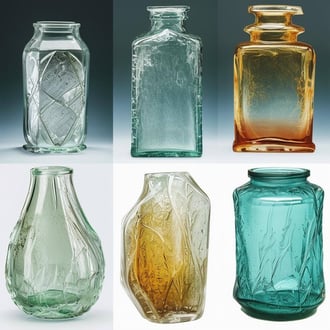
Discover how different types of glass age and degrade over time, and learn how to use AFM technology to investigate ...
11.07.2024
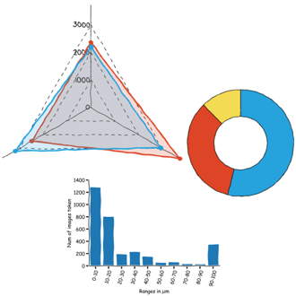
FridayAFM: learn how to perform datamining on large sets of AFM data.
Interested in learning more? If you have any questions, please reach out to us, and speak to an AFM expert.