FlexAFM and nanomotion sensing unveil cellular responses, offering new insights into bacterial behavior and potential ...

24.01.2024
By guest author Alessandro Pitani, Paul-Drude-Institut für Festkörperelektronik, Leibniz-Institut im Forschungsverbund Berlin e. V.
A. Pitanti1,2,3*, M. Yuan1, S. Zanotto3 and P. V. Santos1*
1Paul-Drude-Institut für Festkörperelektronik, Leibniz-Institut im Forschungsverbund Berlin e. V., 5-7, Hausvogteiplatz, Berlin, 10117, Germany
2Dipartimento di Fisica “E. Fermi”, Universit`a di Pisa, Largo B. Pontecorvo 3, I-56127 Pisa, Italy
3NEST, CNR Istituto Nanoscienze and Scuola Normale Superiore, piazza San Silvestro 12, 56127, Pisa, Italy
*Email: alessandro.pitanti@unipi.it, santos@pdi-berlin.de
Link to publication: High-resolution acoustic field mapping of gigahertz phononic crystals with atomic force microscopy.
#Done with a FLEX: The most flexible atomic force microscope for materials research
The last decades have witnessed wide research activities focused on the integration of acoustic technologies in photonic and electronic devices for improving existing functionalities and enabling novel ones. Surface acoustic waves (SAWs) have played a prominent role in this trend: their high frequency, along with their large quality factors in simple delay line configurations, make them very efficient spectral filters and oscillators in telecommunication applications, manifested by their diffuse use in mobile devices.
A more complex manipulation of SAW will show even further achievements and could be leading the transition to the sixth generation of telecommunication technologies: one can imagine, along with an increase in operating frequency, an enhancement of the SAW-embedded data transmission rate through wave manipulation with complex spatial or frequency multiplexing thus allowing simultaneous on-chip operations, such as filtering, on several communication channels. These complex functionalities are already studied in laboratory environment in proof-of-concept experiments, showing exciting results such as acoustic holography [1], negative acoustic refraction [2], as well as several topological effects [3], igniting the effort towards their validation in commercial platforms.
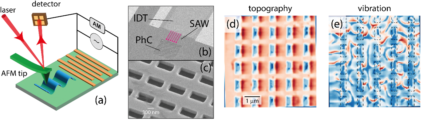
With increasing device frequency and design complexity, the need arises for faster and versatile tools for characterizing acoustic fields at tens of nanometer resolution, improving the existing experimental benches including electrical and optical probes. To this end, we recently demonstrated the implementation of a characterization technique based on atomic force microscopy (AFM) to study the complex wave manipulation properties of phononic crystals (PhC); this is done by measuring the acoustic fields excited by SAWs simultaneously with high-resolution AFM topography (see Ref. [4] for details).
The basic concept behind the so-called Acoustic Atomic Force Microscopy (AAFM) lies in the non-linear interaction between an AFM tip and the sample surface. Given an out-of-plane surface modulation induced by a mechanical wave with amplitude and angular frequency, it is possible to demonstrate that the cantilever deflection “slow” response (as averaged for a time ) carries a contribution coming from the “fast” mechanical wave, despite being the SAW frequency much larger than the inverse of the averaging time :[5]
<d>T=1/κF(z)+1/κ(F''(z)F'(z)/(F'(z)+κ)+F''(z)/2)A2 (1)
Here, is the spring constant and the force-distance curve, and its first and second derivatives, respectively. The second right-hand term in Eq. (1) gives a direct evaluation of the mechanical wave intensity , which can be better extracted by demodulating the mechanical signal under an appropriate amplitude modulation [4] (see Fig. 1 a).
This last step of AAFM technique can be straightforwardly implemented in the Nanosurf FlexAFM, which already includes a secondary lock-in with versatile input-output, in our case used for evaluation of acoustic wave intensity within the very same scan registering sample topography.
Exploiting the fast scanning capabilities of AFM along with the tens of nanometer and below resolution, we characterized GaAs membrane devices with SAW excitation induced via the piezoelectric effect with interdigitated transducers (IDT). A scanning electron microscopy of one of the investigated devices is reported in Fig. 1 (b-c).
We investigated SAW vibrations around 1 GHz in standing wave configuration, assessing their scattering with non-homogeneous interfaces and defects; moreover, we investigated the role of unit cell symmetry for the Bloch modes of PhC in the same frequency range, showing how the patterning induce a strong modification of the density of states resulting in possible, complex manipulation of the mechanical waves.
A typical measurement of a PhC is shown in Figure 1 (d-e). While the topography shows few unit cells comprising rectangular holes in a square lattice on a GaAs membrane, the extracted vibrations exhibit a complex pattern, given by the superposition of multiple, scattering-induced Bloch modes, which can be investigated at a single unit cell level, already overcoming the diffraction-limited lateral resolution of interferometric techniques. More details can be found in [4].
References
[1] M. Xu, W. S. Harley, Z. Ma, P. V. S. Lee, and D. J. Collins, Sound-speed modifying acoustic metasurfaces for acoustic holography, Advanced Materials 35, 2208002 (2023) https://doi.org/10.1002/adma.202208002
[2] S. Zanotto, G. Biasiol, P. Santos, and A. Pitanti, Metamaterial-enabled asymmetric negative refraction of Ghz mechanical waves, Nature Communications 13, 5939 (2019) https://doi.org/10.1038/s41467-022-33652-8
[3] J. Cha, K. Kim, and C. Daraio, Experimental realization of on-chip topological nanoelectromechanical metamaterials, Nature 564, 229 (2018) https://doi.org/10.1038/s41586-018-0764-0
[4] A., M. Yuan, S. Zanotto and P. V. Santos, High-resolution acoustic field mapping of gigahertz phononic crystals with atomic force microscopy, Phys. Rev. Applied 20, 054054 (2023). https://doi.org/10.1103/PhysRevApplied.20.054054
[5] J. Hellemann, F. Müller, M. Msall, P. V. Santos, and S. Ludwig, Determining amplitudes of standing surface acoustic waves via atomic force microscopy, Phys. Rev. Appl. 17, 044024 (2022) https://doi.org/10.1103/PhysRevApplied.17.044024
23.06.2026
FlexAFM and nanomotion sensing unveil cellular responses, offering new insights into bacterial behavior and potential ...

27.05.2026
Explore Alejandro Silhanek’s innovative spintronics research, showcasing how spin waves can be investigated leveraging ...
.jpg?width=330&height=330&length=330&upsize=true&upscale=true&name=Mayfield%20Girls-202581%20(1).jpg)
19.05.2026
A group of young girls from Mayfield school wanted to start a F24 electric car racing team, and Nanosurf decided to ...
18.04.2024
FridayAFM: See how one of our Industrial AFMs can be used to look at the surface of mobile phones.

28.03.2024
Explore the world of AFM experiments with bismuth oxide layers in this blog post. Learn about electrical measurements ...

21.03.2024
FridayAFM: Point contact diode on lead sulfide.
Interested in learning more? If you have any questions, please reach out to us, and speak to an AFM expert.