FlexAFM and nanomotion sensing unveil cellular responses, offering new insights into bacterial behavior and potential ...


02.08.2023
By guest author Nico Budai, Institute for Solid State Physics, The University of Tokyo
Nico Budai1, Hironari Isshiki1,2, and YoshiChika Otani1,2,3*
1Institute for Solid State Physics, The University of Tokyo; Kashiwa, Chiba, 277-8581, Japan.
We have recently developed a novel magnetic imaging method based on thermoelectric conversion and atomic force microscopy [1,2]. The technique is based on atomic force microscopy and the anomalous Nernst effect (ANE). It has a sub-100 nm spatial resolution and is independent of any net magnetization, making it applicable to non-collinear antiferromagnets.
The proposed technique is based on atomic force microscopy and the anomalous Nernst effect (ANE), which converts a temperature gradient of a magnetized sample into a measurable orthogonal electric field. Figure a) provides the schematics of our method. The device to be measured is placed in the Nanosurf CoreAFM, which provides enough space to connect our device with the necessary wiring. The structure consists of the sample itself and an adjacent heating wire which raises the device temperature. If the AFM-tip touches the surface of the heated sample, a local vertical temperature gradient, ∇Tz, is induced (the AFM-tip works here as a heat sink) below the tip-contact area. Due to the magnetization dependence of the anomalous Nernst effect, given by
EANE = SANE ⋅ (m × ∇T)
and the locally induced temperature gradient, the magnetization direction (or anomalous Nernst effect) of the touched point on the sample surface can be detected. Next to Nanosurf's user-friendly interface and the I/O module, it is straightforward and convenient for us to map the measured anomalous Nernst voltage during a typical topographical scan. We also use the variable magnetic field sample holder, which allows us to scan under an external magnetic field without worrying about a more complicated setup. The sample we were investigating was the Weyl ferromagnet Co2MnGa, known for exhibiting a very high anomalous Nernst effect among metals [3]. Figure b) shows the topographical image of our device, including the heating wire. The sample itself is indicated with a white box.
We can scan the change in the sample's magnetization under different external magnetic fields. As indicated in Figure c), a clear difference in magnetic contrast from -80 mT to +50 mT can be seen. Here, blue means a negative measured voltage, and red indicates a positive one, which resembles a negative and positive magnetic field. At 0.05 mT, even a clear domain wall (transition from blue to red in the middle of the wire) can be determined.
Actually, our technique provides a sub-100 nm spatial resolution and does not, as mentioned before, rely on any net magnetization, making this technique a promising candidate in materials science. Non-collinear antiferromagnets have recently achieved wide attention since they exhibit anomalous Hall and Nernst effects despite barely any net magnetization, making them a promising candidate for data storage devices or spintronics applications [4]. Especially for non-collinear antiferromagnets, this magnetic imaging technique can be applied to determine their magnetic domain structure with uncomplicated means.
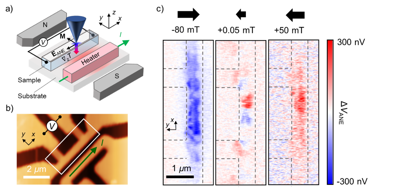
Figure: a) Schematics of the proposed magnetic imaging method based on the anomalous Nernst effect and atomic force microscopy. b) Topographical image of the Co2MnGa sample. The nanopattern is prepared by electron beam lithography. The sample itself, as well as the adjacent heating wire, can be seen. c) Result of the anomalous Nernst effect mapping under different external magnetic fields applied by the variable magnetic field sample holder. The measurement clearly shows the magnetization change inside the sample under the variation of the external magnetic field.
References
[1] N. Budai et al., Appl. Phys. Lett. 122, 102401 (2023)
23.06.2026
FlexAFM and nanomotion sensing unveil cellular responses, offering new insights into bacterial behavior and potential ...

27.05.2026
Explore Alejandro Silhanek’s innovative spintronics research, showcasing how spin waves can be investigated leveraging ...
.jpg?width=330&height=330&length=330&upsize=true&upscale=true&name=Mayfield%20Girls-202581%20(1).jpg)
19.05.2026
A group of young girls from Mayfield school wanted to start a F24 electric car racing team, and Nanosurf decided to ...
Interested in learning more? If you have any questions, please reach out to us, and speak to an AFM expert.