FlexAFM and nanomotion sensing unveil cellular responses, offering new insights into bacterial behavior and potential ...

17.11.2025
Transportation, energy production and healthcare. It is difficult to find a field untouched by material science. Metallurgy, in particular, has always accompanied human history and evolution. Bronze was one of the first alloys ever created, so significant that it gave its name to an entire Age. Thousands of years later, steel powered the Industrial Revolution, and today alloys remain fundamental to electronics. Behind every silicon chip lies a hidden network of metal alloys that make modern technology possible. From aluminum-silicon-copper interconnects that keep signals flowing to titanium and tantalum barriers that prevent atomic diffusion, these engineered blends are essential for semiconductor reliability. Even the chips themselves are evolving, with alloy semiconductors such as silicon-germanium and III-V compounds, formed from elements in the third and fifth groups, like gallium arsenide, indium phosphide and aluminum gallium arsenide, driving faster and more efficient devices for the digital age.
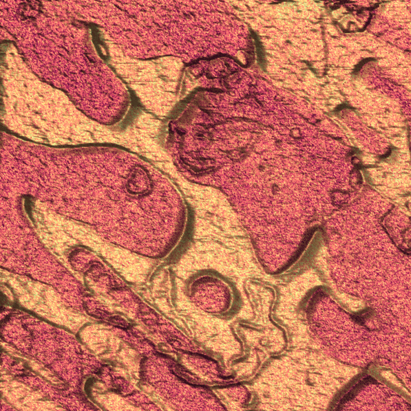
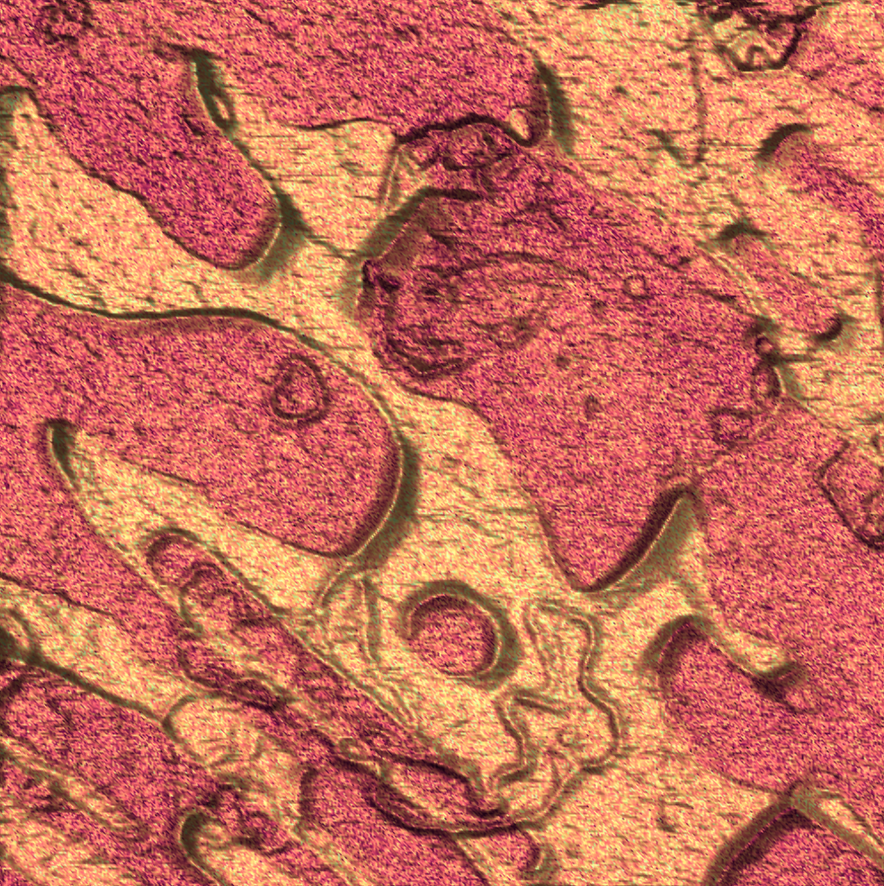
Image of solder tin Sn63Pb37, acquired with DriveAFM on stand-alone material science setup,
resolution: 500 pixel x 500 pixel , scan size: 2 μm x 2 μm.
Today, designing new alloys requires meticulous attention to detail, as they must meet specific requirements for functionality and properties. Mechanical metamaterials, including nano- and micro-architected structures, exhibit characteristics that arise primarily from their geometry rather than their constituent materials. Advances in fabrication techniques have made it possible to create both periodic and disordered architectures, unlocking mechanical behaviors rarely observed in natural materials.
Thanks to tools that allow us to investigate characteristics at the micro- and nanoscale, such as atomic force microscopy (AFM), we can now account for physical properties at these dimensions. The structure of an alloy plays a crucial role in determining its mechanical behavior. Grain and phase boundaries, for example, can restrict the movement of dislocations, influencing plastic deformation. Understanding the arrangement, dominant orientations and scale of phase separation within an alloy is therefore essential for predicting its performance.
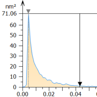
Another common technique for investigating metallic surfaces is nanoindentation, but it is typically quite slow. Nanosurf’s DriveAFM, equipped with CleanDrive photothermal excitation and FastScanning, can scan an area of 1 μm x 1 μm in under 35 s per frame (linerate 15 Hz) at high resolution (512 pixel x 512 pixel) thanks to WaveMode, the fastest off-resonance AFM technique. Moreover, with WaveMode NMA it is possible to directly obtain quantitative elasticity values alongside the usual topography. This makes it straightforward to visualize variations in elasticity, highlighting different phases.
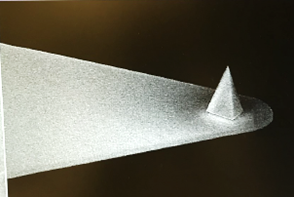
Scanning electron microscope image of a WM20PTD AFM probe used for WaveMode.
With WaveMode NMA, Nanosurf has pushed the boundaries of quantitative measurements on metal alloys, as reported in the peer-reviewed journal SMALL. “The goal of the measurement was to test the upper elasticity range we could access, but indenting metal alloy requires a stiff probe. The stiffer the probe, the more challenging it becomes to drive it through photothermal excitation.” explains Hans Gunstheimer, R&D engineer at Nanosurf and first author of the article. Photothermal excitation in WaveMode is achieved through a second laser focused on the cantilever, which means a stiffer probe requires more laser power to bend. This was made possible through collaboration with an innovative research partner, where a specialized coating for the cantilever was developed. In the study, researchers accurately describe the physics revealed by this method: the motion of the probe under photothermal actuation depends strongly on how heat propagates along its length. Variations in heat distribution across the cantilever lead to different bending patterns, shaping its vertical motion over time and along its span. This understanding is key to fast quantitative nanomechanics without adding complexity. Our Studio software includes everything required for high-resolution, fast, and quantitative measurements, such as all WaveMode NMA controls, quantitative analysis tools, and a one-click calibration workflow. With its intuitive and customizable interface, Studio is easy to use and provides full control over measurements.
23.06.2026
FlexAFM and nanomotion sensing unveil cellular responses, offering new insights into bacterial behavior and potential ...

27.05.2026
Explore Alejandro Silhanek’s innovative spintronics research, showcasing how spin waves can be investigated leveraging ...
.jpg?width=330&height=330&length=330&upsize=true&upscale=true&name=Mayfield%20Girls-202581%20(1).jpg)
19.05.2026
A group of young girls from Mayfield school wanted to start a F24 electric car racing team, and Nanosurf decided to ...

08.12.2024
Learn how to make a Python code to interface your AFM with a gamepad.

01.10.2024
Discover how different types of glass age and degrade over time, and learn how to use AFM technology to investigate ...
02.07.2024
FridayAFM: learn how to automatize data analysis in MountainsSPIP
Interested in learning more? If you have any questions, please reach out to us, and speak to an AFM expert.