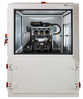
Why Wafer Roughness Matters
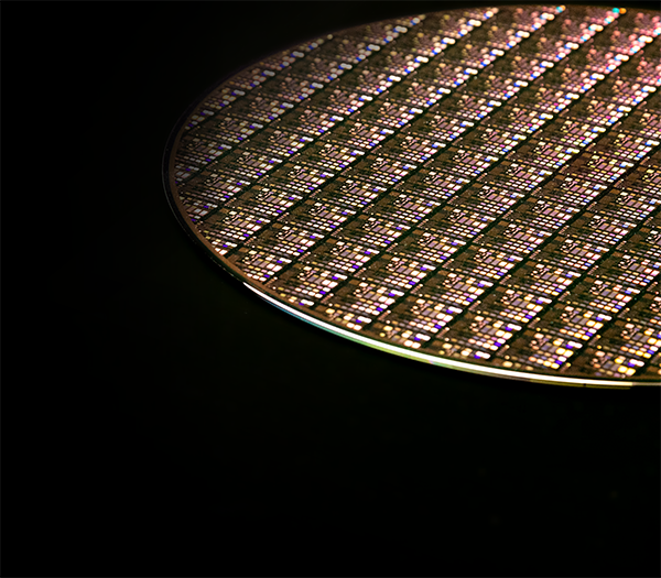
Even tiny irregularities can have a major impact on device performance. Excessive roughness, for instance, can degrade key electrical characteristics by reducing the mobility of electrons and holes, ultimately compromising the efficiency and reliability of the final device. This effect extends far beyond electrical performance, influencing every stage of semiconductor manufacturing, from adhesion and photolithography to overall device reliability.
A rough wafer scatters charge carriers, driving up resistance and cutting efficiency, which might impair high-performance CPUs, GPUs, and memory chips. It also downgrades thin-film adhesion, photolithography precision, and even optical properties in LEDs and solar cells. Worse, roughness can trigger cracks and defects in the material, reducing yield and reliability.
Unmatchable Speed
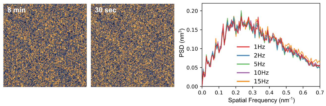
Nanosurf has introduced the unique WaveMode, an off-resonance AFM mode. With its up to 15x speed compared to conventional techniques, it is the fastest off-resonance mode on the market.
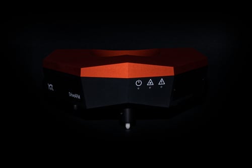
WaveMode is possible thanks to the CleanDrive technology, consisting of a second laser which excites the cantilever off-resonance phototermically; unlike other implementations of off-resonance modes, WaveMode has the advantage that it does neither need nor rely on subtraction of any parasitic background.
The fast scanning capability means higher throughput for applications in the semiconductor industry.
Reproducible and Consistent Results
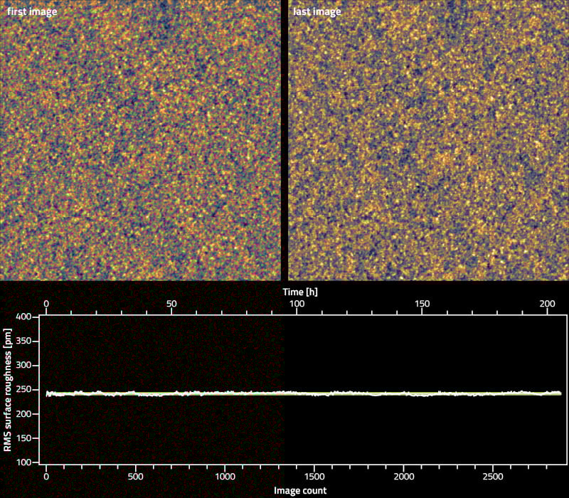
Wavemode, Nanosurf’s advanced photothermal off-resonance mode, delivers outstanding noise performance, ensuring highly accurate surface roughness measurements while maintaining imaging stability and superior quality. Its capability of precisely controlling interaction forces below 1 nN preserves tip sharpness over long periods of time, greatly reducing cost of ownership.
In our dataset, collected over 10 consecutive days, the distribution of measured roughness remains consistent, and this confirms that the tip quality is preserved from start to finish and delivering low noise datasets.

Smarter AFM Workflows with Nanosurf Studio
Nanosurf Studio is the next-generation control and analysis software that brings precision, flexibility, and ease of use to your AFM workflows that transform AFM measurements into a seamless, intuitive process.
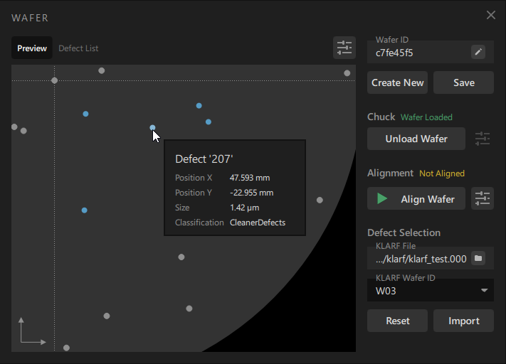
From the very first step, Nanosurf Studio ensures safe and accurate wafer loading with guided procedures that protect your system and guarantee correct placement. Built-in alignment tools deliver accurate positioning, laying the foundation for consistent, high quality measurements.
For routine tasks, automation features let you set up and complete metrology tasks with just a few clicks, while full manual control remains at your fingertips for developing and refining new applications.
KLARF file support allows you to import defect maps and jump directly to the locations that matter most. ViewPort provides a clear, interactive wafer overview, navigation becomes fast, precise, and remarkably user-friendly