Hybrid Bonding and Advanced Packaging
Hybrid bonding operates at the nanometer scale.
At these dimensions, metrology accuracy is the difference between high yield and hidden failure.
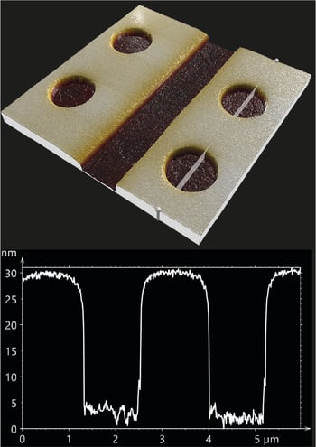
- Nanometer‑level planarity and roughness control
Cu–Cu and dielectric bonding tolerate only a few nanometers of height variation, making ultra‑high vertical resolution essential. - Highly reproducible processes with production relevance
Development of reliable and scalable CMP processes is crucial for hybrid bonding and semiconductor manufacturing - Gentle measurement of fragile surfaces
WaveMode enables true nanometer resolution while minimizing tip–sample forces, preserving sensitive copper and dielectric surfaces.
These requirements make advanced AFM‑based metrology a foundational enabler of reliable, fine‑pitch hybrid bonding.
Sample courtesy: ErzM / Fraunhofer ENAS
Why Metrology in Hybrid Bonding Matters
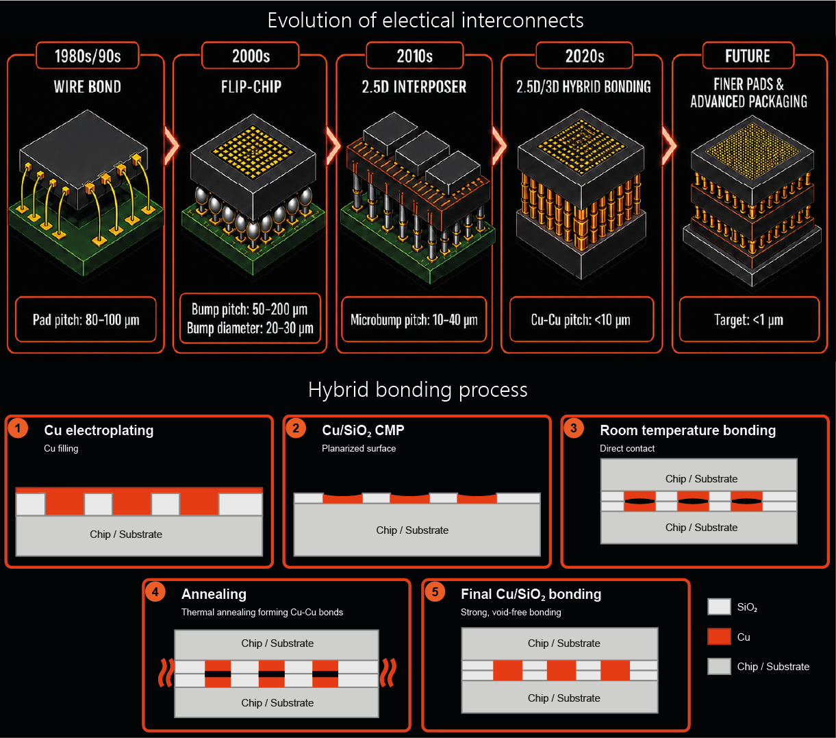
As interconnect pitches approach sub‑micrometer size, hybrid bonding pushes semiconductor manufacturing into a regime where metrology tolerances tighten to the nanometer scale and margins for error disappear. At these dimensions, Cu pads and dielectric surfaces must be exceptionally planar, clean, and precisely aligned, because even a few nanometers of height variation, wafer bow, or residual contamination can prevent reliable Cu–Cu contact and lead to latent yield loss. In this regime, traditional optical inspection alone is no longer sufficient, and AFM becomes indispensable.
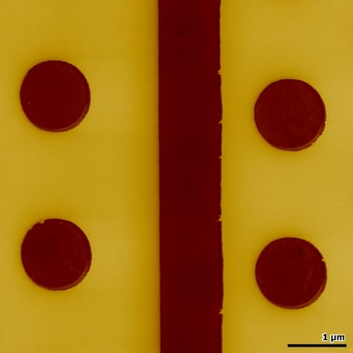
Metrology must measure surface topography with very high vertical and lateral resolution to accurately capture Cu pad dishing and roll‑off. These values are critical for the following bonding steps and must be tightly controlled and optimized. As a result, AFM‑based CMP process control is essential: CMP quality and uniformity directly define bonding performance, and only by minimizing post‑bonding defects such as voids or unbonded regions can yield loss be avoided.
Incredible Accuracy
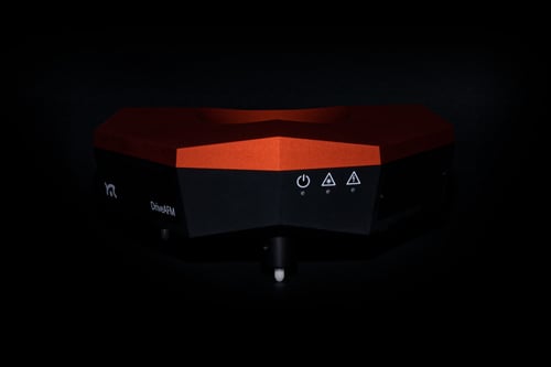
Nanosurf DriveAFM brings atomic‑level clarity to hybrid bonding metrology. With sub‑Ångström vertical resolution, it reveals the smallest topography variations in Cu pads and dielectric layers that determine bonding success at fine pitches. Its ability to reliably probe topography opens a direct window into interfaces critical for hybrid bonding that are not accessible with other surface metrology techniques.
The result is an exceptionally faithful, quantitative view of hybrid bonding features, measured with the accuracy required to push reliable 3D integration to its limits.