FlexAFM and nanomotion sensing unveil cellular responses, offering new insights into bacterial behavior and potential ...


27.05.2026
Discover the instrument behind this story: DriveAFM
We are all familiar with electronics, which rely on the dynamics of electrons and the propagation of electromagnetic waves. However, to achieve low-power computation, high-performance memory devices, and potentially even quantum computers, researchers are also exploring spintronics. In this field, the fundamental elements of logic circuits and memory units are based on the spins of electrons. This is one of the research directions pursued by Alejandro Silhanek, a professor of physics at the University of Liège in Belgium, who specializes in magnetism and superconductivity.
The concept of particle spin is not easy to grasp for those unfamiliar with quantum mechanics. Spin refers to the angular momentum of a particle, a quantity that in classical physics is associated with the rotation of a body. In the quantum realm, this interpretation no longer applies because particles cannot be viewed as tiny spheres; they are better described as probability clouds. Spin is therefore an intrinsic (fundamentally relativistic) property of each particle, which can only take specific values. For electrons, these values are -1/2 or +1/2.
In some solids, under specific conditions, electron spins can synchronize and form spin waves. In spintronics, these waves are generated by applying electromagnetic fields to materials such as permalloy, an alloy composed of 80% nickel and 20% iron, which is highly responsive to external magnetic fields. Spin waves can then be manipulated and measured in ways similar to electromagnetic waves, exploiting effects such as diffraction and interference.
“With spin waves, it is possible to create interference similar to light, blocking their transmission by introducing a hole in the sample and forcing them to follow different paths,” explains Alejandro Silhanek. To investigate this at a fundamental level, researchers in his group fabricated a gap in a permalloy sample to test whether spin waves could pass through it. Intuitively, one would expect that when the permalloy is completely removed, the spin waves would be entirely blocked and unable to cross the gap. “Actually, we found that more spin waves were detected through a complete gap than through a partial gap. The fundamental question we wanted to answer was: why is that? How is it possible that a full gap blocks less?”
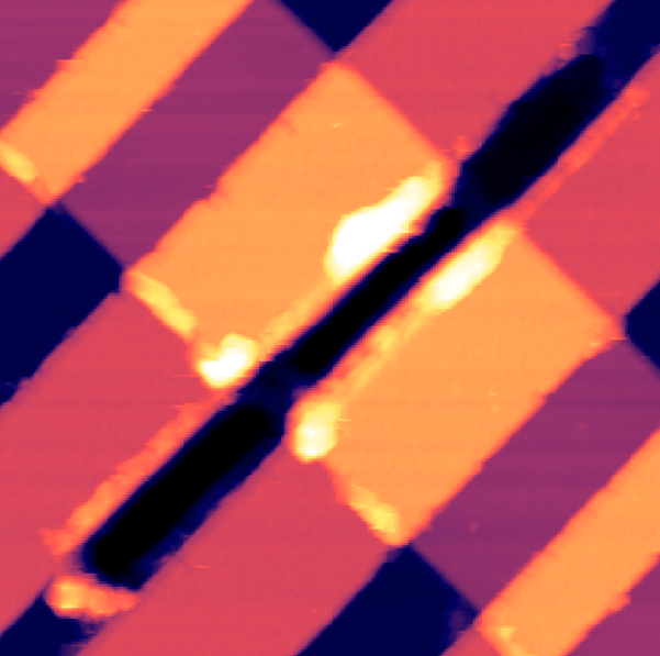
To investigate this question, they used the DriveAFM. This high-end instrument enabled them to perform nanolithography and remove material to create the gap by scratching the surface with a stiff probe. Before they could start digging, researchers had to remove a 50 nm layer of insulating material above the permalloy, then fabricate a 1 μm gap using the AFM. The depth of the gap was gradually increased until the permalloy was completely removed.
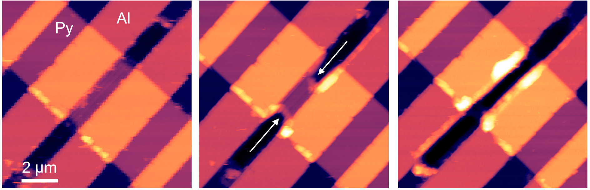
Illustration of the Atomic Force Nanolithography grooving of a Permalloy (Py) stripe embedded between Aluminum (Al) stripes. Material is gradually removed by the mechanical action of the AFM tip, enabling precise control over the groove depth and shape. Courtesy of Alejandro Silhanek / Cyril Delforge, Université de Liège
Through this process, they discovered that the answer lies in the oscillation modes of the spin wave, which describe the wave’s shape at the gap. “In the pristine sample, the cross-section of the wave has a maximum in the middle, like a bump. But if you introduce a defect, you create a destructive-constructive interference pattern and a diffraction pattern, which results in a different oscillation mode. Across the gap, this leads to lower detected intensity,” explains Cyril Delforge, first author of the study and a PhD candidate in Silhanek’s lab.

Sequence showing propagating spin wave spectroscopy (PSWS) measurement protocol: AFM lithography of a groove, AFM imaging of the patterned groove, and the resulting impact of the groove on spin‑wave propagation. Orange arrows indicate the spin-waves, while green regions highlight the detection zones for the AC magnetic flux generated by the propagating waves. Courtesy of Alejandro Silhanek / Cyril Delforge, Université de Liège
Compared to other technologies, AFM offers unique advantages for performing nanolithography, such as the ability to iteratively remove material from the same sample with high accuracy. In contrast, electron-beam lithography using lift-off based processing provides higher throughput but lacks sufficient precision, and variability from sample to sample is too high. “With electron beam lithography, there is a lot of unwanted or uncontrolled nanolithography, so comparisons become meaningless because the data scatter is very large. Instead, you need to take a single sample and modify it with AFM.” Ion beams also presented some drawbacks for this experiment, as they leave residues of gallium ions.
Alejandro Silhanek’s laboratory also has expertise in low-temperature physics, using cryostats to reach temperatures as low as 4 K (around -269 °C). They employ optical and electrical microscopes to observe and characterize their samples. To detect magnetic fields on the sample surface, Silhanek and his team use magnetic force microscopy, which measures gradients of the magnetic field across the surface.
23.06.2026
FlexAFM and nanomotion sensing unveil cellular responses, offering new insights into bacterial behavior and potential ...

27.05.2026
Explore Alejandro Silhanek’s innovative spintronics research, showcasing how spin waves can be investigated leveraging ...
.jpg?width=330&height=330&length=330&upsize=true&upscale=true&name=Mayfield%20Girls-202581%20(1).jpg)
19.05.2026
A group of young girls from Mayfield school wanted to start a F24 electric car racing team, and Nanosurf decided to ...
11.07.2024
FridayAFM: learn how to perform datamining on large sets of AFM data.
02.07.2024
FridayAFM: learn how to automatize data analysis in MountainsSPIP
26.06.2024
FridayAFM: learn how AFM makes possible modern ball point pens.
Interested in learning more? If you have any questions, please reach out to us, and speak to an AFM expert.